
Upgrade Amiga 500 rev. 8a board to Amiga 500+
A while ago I got an empty Amiga 500 plus (+) case, without keyboard and mainboard. I had a spare Amiga 500 rev.8a board (and keyboard), so I decided tot upgrade that one to an Amiga 500+. In this post I show which components must be replace on the board and which changes must be done to the board.
The board before the upgrade

Components to do the upgrade
| Position | Component |
| U19 | DRAM 256K x 4bit 120ns |
| U18 | DRAM 256K x 4bit 120ns |
| U17 | DRAM 256K x 4bit 120ns |
| U16 | DRAM 256K x 4bit 120ns |
| U32 | 74F139 |
| U9 | Oki MSM6242B (RealTimeClock) |
| Y9 | Crystal 32.768Hz |
| TC9 | Trim capacitor 6.8 – 45pF |
| C9 | Axial 0.33uF (330nF) capacitor |
| C911 | 22pF capacitor |
| C913 | Tantalum radial 4,7uF / 16V capacitor (I used electrolytic capacitor) |
| R911 | 470 Ohm resistor |
| R913 | 470 Ohm resistor |
| R914 | 10K Ohm resistor |
| D911 | 1N914 / 1N4148 diode |
| D912 | 1N914 / 1N4148 diode |
| BT9 | CR2032 battery (with adaptor) if needed |
Memory
Components needed: U19, U18, U17, U16, U32


First remove the solder from the holes, and place sockets (low profile) or memory to the board.
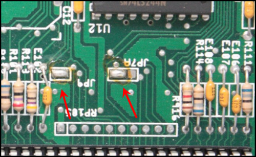
CAS signals (U32)


Remove the solder from the holes, and remove the blobs from the two jumper pads.
Clock circuit


Place components: R914, C911, C9, Y9, TC9, U9

Place components: R911, R913, D911, D912, C913
Note from Sylversio (see comments):
You just placed the components up, without considering that this PCB Schema is wrong, Where R913 should be replaced by a Diode, and D912 cathode should be connected to cathode of the new diode placed in R913 (that both connected electrically with + C913.
Otherwise you could damage your board.
Also, mention to … oscillator… should not be solder the chassis to the board.
All that become from a mistake in A500 rev8 board, that didn’t routed properly the tracks from Schema.
Change / remove jumper blobs
JP2 setting
 Original setting |
 New setting |
JP7A & JP9 setting
 Original setting |
 New setting |
Finished board

The complete machine

10 comments